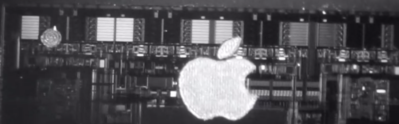
If you want to see inside an integrated circuit (IC), you generally have to take the die out of the package, which can be technically challenging and often destroys the device. Looking to improve the situation, [Bunnie] has been working on Infra-Red, In Situ (IRIS) inspection of silicon devices. The technique relies on the fact that newer packages expose the backside of the silicon die and that silicon is invisible to IR light. The IR reflects off the bottom metalization layer and you can get a pretty good idea of what’s going on inside the chip, under the right circumstances.
As you might expect, the resolution isn’t what you’d get from, say, a scanning electron microscope or other techniques. However, using IR is reasonably cheap and doesn’t require removal from the PCB. That means you can image exactly the part that is in the device, without removing it. Of course, you need an IR-sensitive camera, which is about any camera these days if you remove the IR filter from it. You also need an IR source which isn’t very hard to do these days, either.
Do you need the capability to peer inside your ICs? You might not. But if you do and you can live with the limitations of this method, it would be a very inexpensive way to get a glimpse behind the curtain.
If you want to try the old-fashioned way, we can help. Just don’t expect to be as good as [Ken] at doing it right away.
Source: https://hackaday.com/2023/03/09/bunnie-peeks-inside-ics-with-ir/