News: Microelectronics
14 November 2023
In collaboration with Shin-Etsu Chemical Co Ltd, Tokyo-based Oki Electric Industry Co Ltd has developed technology that uses its CFB (crystal film bonding) technology to lift off only the gallium nitride (GaN) functional layer from Shin-Etsu Chemical’s QST (Qromis Substrate Technology) substrate (a composite material substrate developed by California-based Qromis Inc and licensed exclusively for GaN growth to Shin-Etsu in 2019) and bond it to a different material substrate.
The technology enables the vertical conduction of GaN and is expected to contribute to the realization and commercialization of vertical GaN power devices capable of controlling large currents. The two firms will work further together to develop vertical GaN power devices that can be implemented by partnering with companies that manufacture these devices.
GaN devices combine high-performance device characteristics with low power consumption, such as power devices that require high breakdown voltages of 1800V or more, high-frequency devices for Beyond5G, and high-brightness micro-LED displays. In particular, demand for vertical GaN power devices is expected to grow significantly as they can improve the basic performance of electric vehicles by enabling extended driving ranges and shortened power supply times. However, two major challenges hinder the implementation of vertical GaN power devices: the diameter of the wafers must be increased to improve productivity and vertical conductivity must be realized to enable large current control.
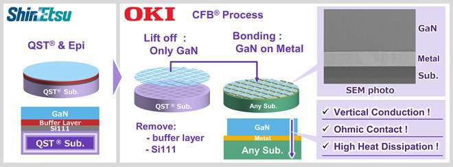
Picture: An overview of the new jointly developed technology.
The coefficient of thermal expansion of Shin-Etsu Chemical’s QST substrate is equivalent to that of GaN, so it can suppress warpage and cracking. This enables the crystal growth of thick GaN films with high breakdown voltages even on wafers larger than 8-inches, enabling the production of wafers with larger diameters.
In addition, OKI’s CFB technology can lift off just the GaN functional layer from the QST substrate while maintaining high device performance characteristics. The insulating buffer layer required for GaN crystal growth can be removed and bonded to various substrates via metal electrodes that allow ohmic contact. Bonding of these functional layers to a conductive substrate with high heat dissipation will enable both high heat dissipation and vertical conductivity. It is reckoned that the combined technologies of Shin-Etsu Chemical and OKI can hence solve the above two major challenges, paving the way for the implementation of vertical GaN power devices.
In the future, the two companies aim to contribute to the widespread use of vertical GaN power devices through Shin-Etsu Chemical’s provision of QST substrates or GaN grown QST substrates to companies manufacturing GaN devices and OKI’s provision of CFB technology through partnering and licensing. Furthermore, OKI hopes to use CFB technology to provide added value to semiconductor devices that go beyond the framework of single materials.
Shin-Etsu Chemical launches QST substrates for GaN power device growth
Shin-Etsu licenses Qromis’ GaN substrate technology
Source: https://www.semiconductor-today.com/news_items/2023/nov/oki-shinetsu-141123.shtml