The ferroelectrical properties of materials have found a variety of uses over the years, including in semiconductor applications. Ferroelectric memory is among the most interesting and possibly world-changing as it could replace today’s fragile and (relatively) slow NAND Flash with something that’s more robust and scalable. Yet as with any good idea, finding the right materials and process to implement it is half the battle. Here is where a recently released paper in Advanced Science by Shurong Miao and colleagues demonstrates a FeFET-based memory cell design using α-In2Se3 material on platinum-based source-drain electrodes.
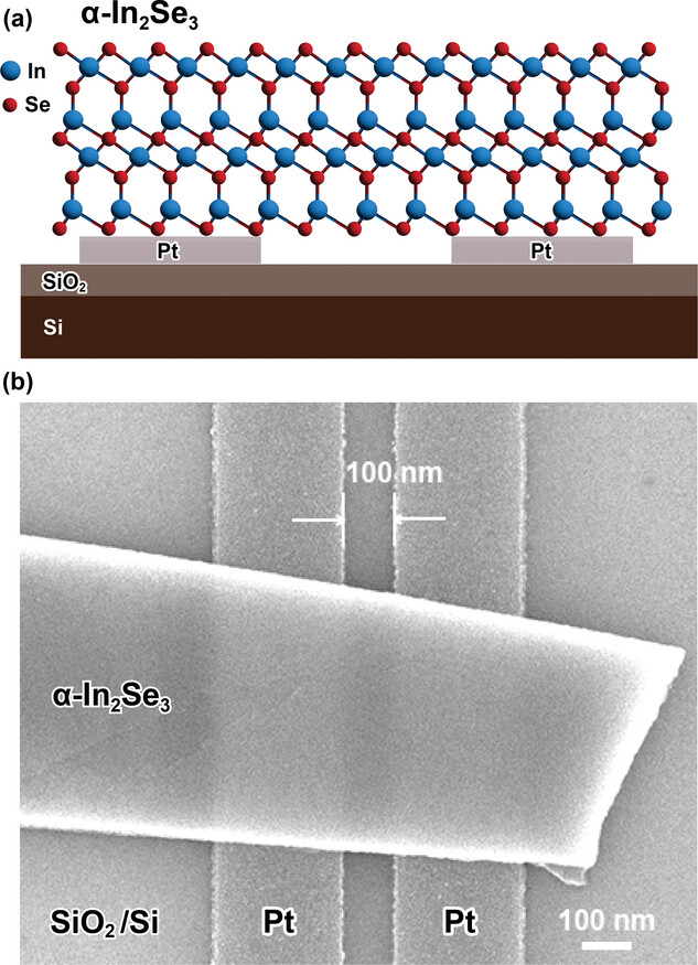 Schematic and SEM image of α-In2Se3-based FeFET. (Credit: Miao et al., 2023)
Important to note here is that FeFET (ferroelectric field-effect transistor) is distinct from FeRAM, with the latter having a DRAM-like structure whereby ferroelectric material takes the place of the capacitor in traditional DRAM. Such FeRAM has been commercially available since the mid-1990s, with applications including the storing of save states in Sega game console cartridges. FeRAM has benefits over NAND Flash in that it has far higher endurance, but it does not scale to smaller sizes that well, which keeps capacity of FeRAM chips low and thus relatively expensive.
Compared to DRAM, FeRAM is far more power efficient as it retains stored information even when left unpowered, yet it shares the same issue of destructive reads, which necessitates complex write cycles following each read. This is where FeFET-based storage offers many advantages, as the ferroelectric gate material allows a non-destructive read, since what is being read is the effective resistance which depends on whether the gate material is in-plane (IP) or out-of-plane (OOP). Switching the plane orientation is performed in this specific demonstration using +5 V and -5 V, with the read voltage being 0.5 V, well below the coercive voltage that would make it destructive.
What’s interesting here is that the insulator is standard SiO2/Si material, making it compatible with existing semiconductor manufacturing technique. The demonstrated FeFET cell featured a sliver of gate material from an externally grown crystal. Since FeFETs can be expected to scale as well as MOSFETs, the only significant limitation would then appear to be the ferroelectric limit, i.e. the size where a material ceases to be ferroelectric.
Naturally, for such FeFETs to be viable long-term storage and/or DRAM replacements, they need to demonstrate the necessary qualities. In the demonstration by Miao et al., they found that the device lasted for 1200 read/write cycles and retaining data for 17 hours without noticeable degradation. This suggests that the IP/OOP state is quite stable in this gate material and clears the used manufacturing method for further testing. Although FeFET-based memory is probably a while off from large-scale commercialization, these advances give hope that this day won’t be far off now.