Disaggregating chips into specialized processors, memories, and architectures is becoming necessary for continued improvements in performance and power, but it’s also contributing to unusual and often unpredictable errors in hardware that are extremely difficult to find.
The sources of those errors can include anything from timing errors in a particular sequence, to gaps in bonds between chips in a package. And they can change over time as circuits in different chips or chiplets age at varying rates, and as various types of stress turn latent defects turn into real defects. As a result, computations may produce wrong results sometimes — but not every time. That will not be noticeable if one result in an internet search is wrong or if there is a slight glitch in a streaming video, but it takes on a whole different level of importance when it involves financial transactions, automotive safety, or military drone guidance systems.
These types of problems are not entirely new. Technical papers on the subject began appearing in the early 2000s, discussing unexpected behaviors and occasional faults in chips. However, they now have reached a tipping point where the problems are significant enough, and numerous enough, to warrant attention. But what to do about them isn’t always clear, for a number of reasons. Among them:
- There are many more components packed densely onto chips and into packages, some with thinner metal layers and dielectrics, and many more interconnects. That makes it difficult to predict where process variation, latent and real defects, and even quantum effects will cause problems, or in what sequence.
- Advanced-node chips are being used in systems with higher utilization rates than in the past, particularly in data centers and AI applications. That increases the mechanical and electrical stresses on those devices, which can impact signal quality and affect timing. Alongside of that, some of these systems are being designed for longer lifecycles, requiring regular software updates that may cause some hardware components to behave differently over time.
- Designs are becoming more heterogeneous and more customized, increasing the number of possible interactions that are unique to a particular device. In addition, these devices increasingly are using components developed at different process nodes, sometimes manufactured by different foundries, not all of which are characterized equally — or in the context for how they will be used.
All of this adds complexity, making it far more difficult, time-consuming, and expensive to document all the corner cases.
“There are questions about whether these things we’re observing now are because we have a combination of bigger chips and better instrumentation, or whether this is some new thing,” said Rob Aitken, a Synopsys fellow. “In either case, is this something that can be identified at manufacturing time, or will the act of identifying it affect economic yield? I was on a panel recently with someone from IBM, and he said that’s why mainframes are so expensive. They’re designed to look for every single possible problem.”
The open question is whether that will become a requirement for safety-critical and mission-critical hardware. And if so, what is the best way to address it. If everything has to be perfect, that will have an impact on yield and cost. But if some of this can be dealt with by designing resiliency into systems, it could help keep costs under control. There are efforts underway in both directions.
Perfection vs. resilience
The University of Iowa, Baidu Security, and Argonne National Laboratory teamed up to create MinpSID (multi-input-hardened selective instruction duplication), which identifies “elusive error propagation across multiple inputs.” In a newly released technical paper, the researchers claim to have found a way to improve reliability and identify “incubative instructions” that cause these errors.


Fig. 1: Incubative instructions example. Source: Argonne National Laboratory/University of Iowa/Baidu Security
That’s one piece of this puzzle. But so far, there is no single repeatable solution, and it’s not obvious there ever will be. In fact, solutions may be design-specific, and sometimes even counter-intuitive.
“We saw one case in which people were building circuitry where, under certain circumstances, you could do a statistical analysis across different combinations of computation and sometimes get this error,” said Barry Pangrle, power architect at Movellus. “What they were doing was pushing down the voltage. They knew it wasn’t going to meet timing all the time, and what it would come up with were essentially were false positives. They used that as a filter to find the good results, and took that smaller set and ran it on a really robust system. The problem now is everything is getting more complex. As circuits get older, they tend to slow down. So now, from a wellness standpoint, we need to look at aging technology, monitor things, have delay loops and stuff like that, to see if it’s drifting over time.”
Preventing these kinds of sporadic errors requires understanding where they come from in the first place. But with customized collections of chips or chiplets and unique architectures rolling out at an accelerated pace, that’s a non-trivial exercise, which can push up the overall cost of development. And while some of these problems can be addressed after-the-fact with software, it’s much more effective if the hardware itself is programmable. That adds a level of resilience into a design to adjust to any problems without the power/performance hit from fixing problems in software.
“The first thing is detecting when things will go wrong, before they go wrong,” said Geoff Tate, CEO of Flex Logix. “The second thing is doing something about it. If something goes wrong, you need to compensate — just like the human brain. The brain has neurons dying all the time, but our pathways can regenerate. People can have very substantial damage to their brain, but other parts of the brain can get reprogrammed over time to make up for it. Existing chips don’t work that way. The only thing that can make up for it is the processor or the FPGA — something that can be programmed to do something differently.”
Figuring out when and why errors will crop up is time well spent, but in some cases that can mean a lot of time. The silent data errors detected by Google and Meta took more than a year to trace back to the root cause. And frequently problems don’t show up until an entire chip or package is developed, or in use in the field.
“There’s challenges in all the physical mechanics of building this stuff and putting it together in devices,” said Simon Davidmann, CEO of Imperas Software. “There also are challenges as an industry for how do you validate the whole thing when it’s running. We’ve just started collaborating with some companies on the SoC level, and then it will get to the system level. But it’s a long, slow process involving systems of systems.”
Whatever can be done up front to ferret out potential problems is beneficial, and that can involve both physical and virtual factors.
“Thermal analysis plays into that,” said Niels Faché, vice president and general manager at Keysight. “If you have hot spots on the board and in an IC, over time it will have an impact on the performance of the device and contribute to its breakdown. We see more and more emphasis on thermal analysis, and we’ve added thermal modeling to that, because that can change electrical performance. It could be the same with mechanical analysis. You might have a deformation in the board that changes the electrical parameters.”
Heat poses a serious challenge to how a chip or system behaves. “You have to keep an eye on the thermal gradients,” said Marc Swinnen, director of product marketing for the Semiconductor Division of Ansys. “That gives a differential expansion. Even if there’s only a 25° difference between the top and the bottom of a stack, given the extreme thinness of these devices, we’re talking about 10,000° per centimeter or something in that range. It’s a huge temperature gradient for such a small distance, and that leads to quite intense stresses.”
Manufacturing and packaging defects
Not all errors are due to design. They can be caused by any combination of factors at any point in the design through manufacturing flow. In fact, they may show up as latent defects that are considered benign, such as a nanoscale imperfection, or it may be a defect that is overlooked in inspection and test. And some of those defects may not show up until a device begins to age.
“Especially now at 5nm, aging is affecting the timing, and so you’ve got these models of how it will age,” said Kam Kittrell, vice president of product management in the Digital & Signoff Group at Cadence. “But how do you know how it will age until it’s been out there for five years? This means you’ve got to double check things like this. Also, if you find a peculiar case that is failing — maybe a soft failure like a bit flipping every once in a while — that’s not a manufacturing defect, but there’s something you can do at manufacturing test. You can go back and re-do your manufacturing tests with known bad die, and then also disperse that test out to every unit to see if there are some weak links in the chain. There’s lots of goodness that comes from that. Cloud computing is driving this along with automotive, because the complexity of what’s going into automotive is off the charts now. There are supercomputers running in your dashboard everywhere, and people are upset when their car doesn’t work.”
To make matters worse, as chips or chiplets are introduced and stacked in advanced packages and heavily utilized, or as any of these devices are used in ways for which they were not originally designed, latent defects can turn into real defects. Not all of those can be fixed, but they can be identified before they become problematic.
“Latent defects are more about thermo-mechanical aspects,” said Nir Sever, senior director of business development at proteanTecs. “Microbumps can have cracks or voids. Lanes can have bridge shorts. And TSVs can have cracks, partial fills, or sidewall delamination. There are many physical defects happening because the dies are not perfect. But even if they are perfect, when you start the assembly process, there are a lot of potential failure points. In a typical HBM there are about 10,000 different lanes. If one of them is defective, that SiP will not work unless it is repaired. So you have put down all those microbumps, and you have to assemble them so they all touch. If just one of them is defective, a die is warped, or the material moved a little bit and it’s not fully aligned, you will get resistive behavior that will affect the signal quality.”
The challenge is figuring out where and when that might happen, and how to accurately identify problems.
“So first you must be able to test, because yield is not 100%,” Sever said. “There is a good chance that at least one lane will be defective after assembly. Second, because it is aging, you need to keep monitoring the interface throughout the lifetime of the product, in field and in mission mode. If it was marginal from the start, because there was a latent defect that did not generate a test failure, as time goes by it will degrade. Eventually, the timing margin or the eye diagram will start to close and you will get errors on the bus. And that’s a disaster, because unlike in a SERDES where you have error correction mechanisms, in typical D2D you don’t. There is no error correction necessarily built into the protocol. You’re assuming a bit error rate that is virtually zero, like a regular I/O. And that will lead to data errors that manifest in silent data corruption, where nobody really knows where they’re coming from. But the fact is, data is starting to get corrupted somewhere inside the chip, and you must have a way to take measurements from inside, visualize the data, understand it, and then be able to track root causes and fix it.”
Toward more resilience
This is where resilience comes into the picture, and the memory sector has been well out in front on this. For instance, it’s well known that NAND flash degrades over time. You can only write to flash so much before it no longer works.
“There are wear-leveling algorithms that put 30% more bits in there, so that over 10 years they can make it work reliably,” said Flex Logix’s Tate. “But they’ve got to find the bits before they go bad, and then swap in bits that are still good. For resilient [logic] design, you’re going to need something like embedded FPGA, where you’ve got some available unprogrammed compute capacity that can take up whatever it is that’s failing in the rest of the system. All chips have bugs. There are bugs that kill the chip so it doesn’t work. There are bugs that make it so that performance is bad, so it can’t be shipped. And then there are all sorts of bugs you can work around. In our chip, we had a bug that we couldn’t have worked around, except for the fact that we had 4,000 lookup tables of embedded FPGA on the processor bus. We were able to code some RTL on that lookup table that made up for the bug in the rest of the chip. We could then ship the chip and the customer had no idea that we patched it that way.”
Most resiliency solutions rely on some level of redundancy. That can include programmability, which reduces the need for entirely new circuitry, and it can include software, which is inefficient but easy and relatively inexpensive to reprogram. In all cases, there is some overhead. The key is to keep that down to a minimum while choosing which tradeoffs to make in power, performance, and area/cost. So if area/cost is critical, adding in-circuit monitoring can take the place of added circuitry. If power is critical, that redundancy may come in the form of reprogrammable logic. And if performance is the most critical factor, additional circuitry can be added and dynamically turned on and off, depending on where problems arise.
“That’s a question of economics ultimately,” said Richard Oxland, product manager for Tessent Embedded Analytics at Siemens Digital Industries Software. “Are silent data errors costing us more than the cost of the silicon to have redundant compute? That’s a question most semiconductor companies won’t be able to answer because it’s a system-level question. It needs significantly better understanding of the economic impact of silent data errors. And that starts to become very highly proprietary information quite quickly if you think about Meta or Google or AWS. These guys will start to drive down these kinds of requirements if it becomes meaningful. And we might not always get to know that, because they’re designing their own chips. So in your system, you can have some redundancy there. Or in the NoC, you can do smart things like routing to avoid issues.”


Fig. 2: Redundancy and self-testing. Source: Siemens EDA
That adds another level of complexity, though, because there isn’t just one NoC in complex designs. There can be many, and they need to be viewed in the context of the entire system. “Then you have to start dealing with timing between NoCs because they’re not fully synchronized,” said Frank Schirrmeister, vice president of solutions and business development at Arteris IP. “You’ve got to deal with the timing of peripheral connections, and all kinds of clock-domain crossing.”
Adding resiliency into that picture is a challenge, but it’s easier to make the individual pieces resilient using a divide-and-conquer strategy rather than trying to solve the whole problem at once, said Schirrmeister. “You don’t want to deal with a bunch of signals all at the same time. So if you’re looking at safety instructions, for example, you add in checkers to make sure it’s functioning properly.”
Resiliency is getting a lot of attention is in the automotive sector, where chips are being used in safety-critical applications and where regulations require failover of some sort. “The automotive industry always has been very enthusiastic about the reliability of their semiconductors,” Oxland said. “Some of the big suppliers there have been active in that space for a while, like NXP and the like – are very good at this kind of thing. That application may be a slightly lower level of complexity, because we’re talking about ECUs. But generally speaking, these are deployed in huge numbers — although they’re a little bit more deterministic in terms of how they’re operating. We’re seeing the problem with silent data errors now because of the complexities of running very highly parallelized workloads at huge scale, so it’s more of a new problem. We have to approach it by improving how we do traditional things, as well as finding new ways of doing things.”
Tradeoffs at the extreme
When Cerebras developed its wafer-scale chip, it recognized that nothing would yield 100%, and that some parts of the chip — an 800mm² square cut out of a full wafer — would age differently than other parts and that latent defects would turn into real defects.
“Historically, the way DRAM achieved very high yield was to have redundant rows and columns of bit cells,” said Andrew Feldman, Cerebras’ CEO. “We have 850,000 identical programmable elements, which is a core plus memory plus a little router. It’s tied to the next one with wires. And each programmable element is tied to each of its four neighbors, and to its neighbors’ neighbors with a redundant link that allows it to speak to its neighbors. What we did was build a test chip, and we worked with TSMC on their yield data. And what you should have, if the foundry is working within control, is a random distribution of flaws. With that, redundancy should allow you to map out the flaws. So when we say we have 850,000 cores, we actually have 870,000 or so cores, because we’re going to hold about 1.5% aside.”

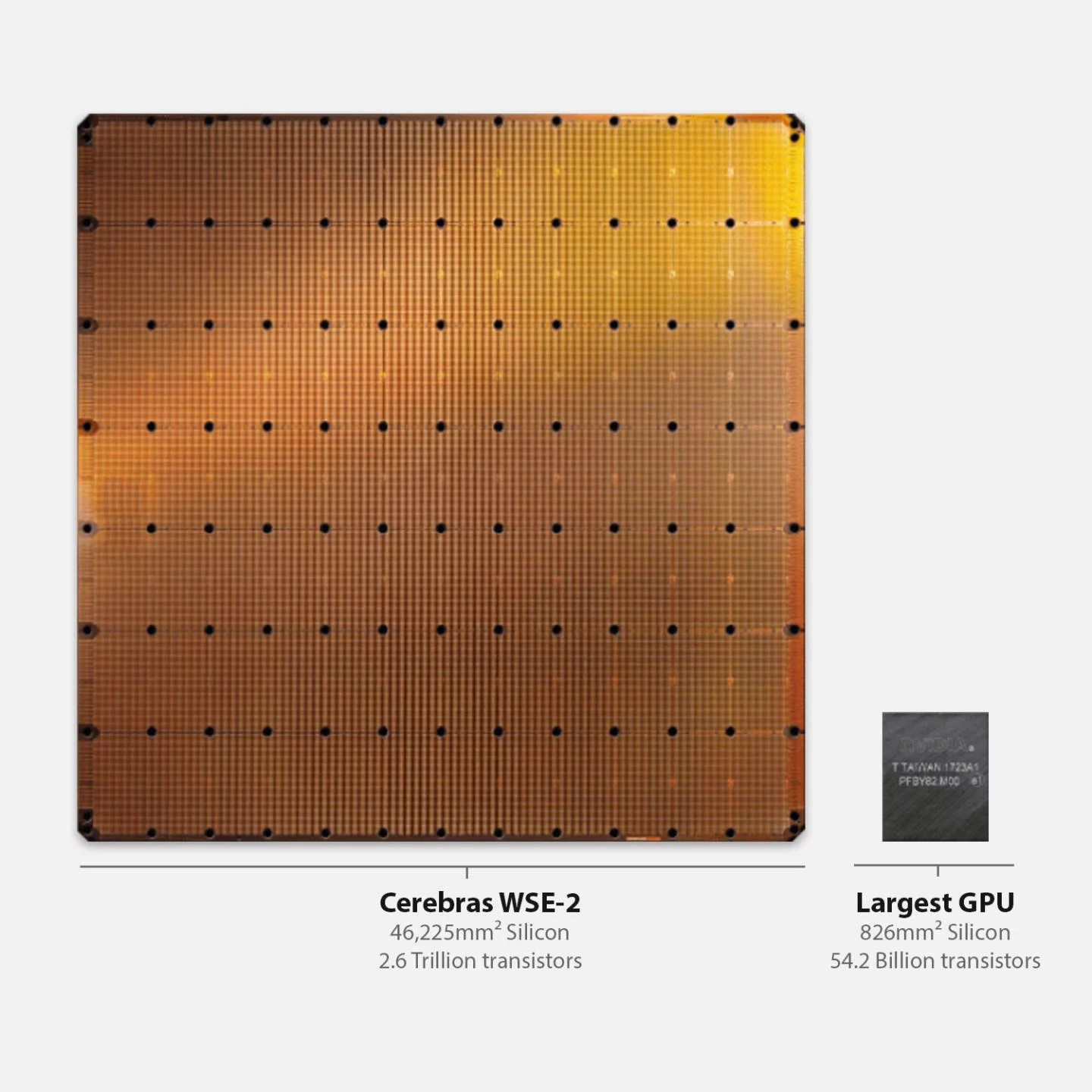
Fig. 3: Wafer-scale chip builds in about 1.5% redundancy. Source: Cerebras
Feldman said other key pieces are to burn in before mapping out, and exposing chips to temperatures that are outside of the specification. “And from there, self-test checks the behavior of every core and every wire between every core,” he said. “If it fails, it activates a route-around protocol and re-does the self-test. So there’s a hardware self-test that runs at bring-up, and then periodically thereafter.”
While this remains impractical for most applications, it does prove a point. With enough effort and innovation, most of these problems can be solved. The challenge is to determine the acceptable tradeoffs for an application, and then to really understand what those tradeoffs actually entail. Not all of that is obvious in today’s hardware and system design.
Conclusion
All of this points to a much broader issue, namely that as complexity continues to increase with denser circuits, more customization and functionality, new materials, and different usage patterns. As a result, the number of unknowns is exploding. Not all of those can be fully understood or debugged, and for many applications that’s okay. But for mission-critical and safety-critical applications, planning for failures is essential.
It’s impossible to catch everything within tight market windows, but with enough time and effort, it appears that chips can be created to withstand most problems. There is no question about the need to build resilience into more chips. It’s a matter of how to achieve enough resilience at a price point that’s acceptable. The chip industry is just starting to take a serious look at this issue.
Source: https://semiengineering.com/how-to-build-resilience-into-chips/